MAI developed cost-saving technology of the production of printed circuit boards
Experts of Moscow Aviation Institute developed a new technology of the production of printed circuit boards, which differs from the existing ones by its efficiency and high precision in the reproduction of the conductive pattern. The efficiency of the technology was tested and proven in the laboratory.
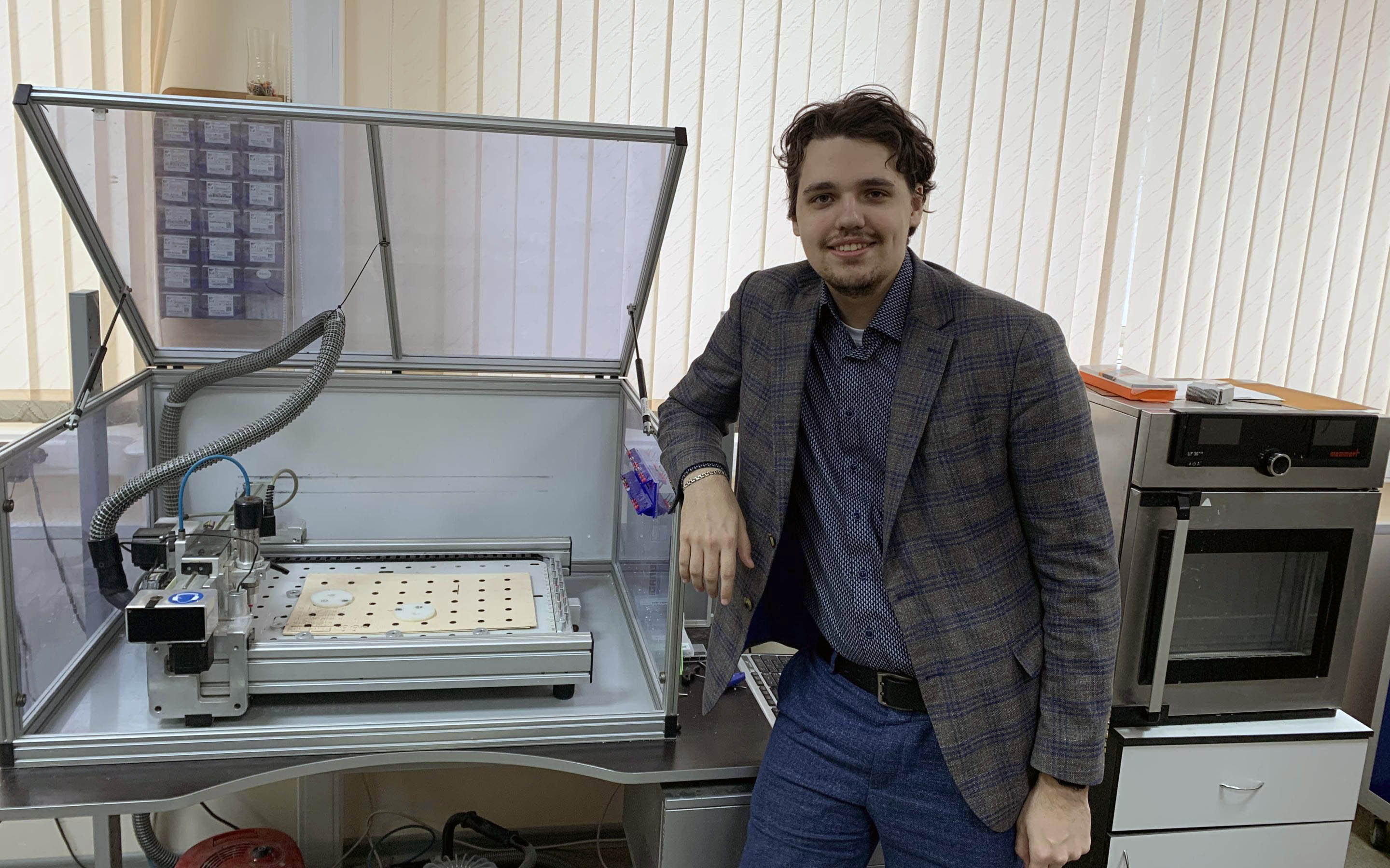
The work is carried out at the department 307 "Digital technologies and information systems" of Moscow Aviation Institute. The initiator of the project is the engineer of the research department of the department Maxim Korobkov, the supervisor is associate professor Olga Khomutskaya.
– Currently, for the production of printed circuit boards, two exposure technologies are used, which make it possible to form a mask on the workpiece for selective etching of the copper layer. With contact technology, selective transmission of ultraviolet light occurs due to a photomask – a conductive board pattern printed on a transparent film. The direct technology involves the impact on the photoresist on the board with a laser beam, – says Maxim Korobkov.
Low cost is characteristic to the first method, but has a number of limitations that affect the quality of the product. The second one gives high accuracy, but direct exposure setups have complex optical and mechanical systems, which makes them very expensive. The technology combines the advantages of existing methods. It involves the selective transmission of light through a liquid crystal matrix – such as is used in the screens of modern monitors. A similar process is used in 3D printing, namely masked stereolithography (MSLA) technology.
– MSLA 3D printing technology is based on the use of an optical system consisting of an ultraviolet radiation source and a liquid crystal matrix. An image of the layers of the manufactured model is sequentially displayed on the LCD screen. The photopolymerizable composition cures under the action of ultraviolet light passing through the matrix. Then the moving platform with the layer formed on it rises to polymerize the next layer. The same principle can be used in the production of printed circuit boards: to influence the workpiece with ultraviolet light passing through the matrix, on which the image of the conductive pattern is located, says the initiator of the project.
At present, a laboratory sample was assembled, on which the fundamental operability of the technology has been confirmed, and the optimal design and technological parameters have been determined. By the end of the year, it is planned to finalize the prototype to a ready-to-use sample.
– Technology makes it possible to speed up the process of manufacturing electronic devices, given that they are becoming more and more complex and smaller. This is an integral part of the development of an electronic database within the framework of Industry 4.0 and digital transformation, – notes Olga Khomutskaya.
Previously, the project received prizes at the International Youth Scientific Conference "Gagarin's Readings" and the competition of scientific and technical works and projects "Youth and the Future of Aviation and Cosmonautics". Scientists are confident that the new technology will be in demand in laboratories and enterprises involved in the design of electronics.


